
RTL Design & Verification
VHDL, Verilog and SystemVerilog RTL development with directed and constrained-random verification using C/C++, SystemVerilog and UVM.
Digital ASIC and SoC engineering from architecture and RTL through synthesis, DFT, physical implementation and sign-off.
ANKASYS supports teams where specialist implementation capability is needed, from early RTL decisions to physical implementation and verification closure.
REAL ENGINEERING CONTEXT
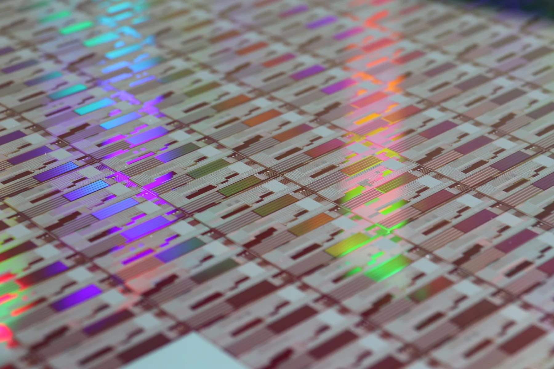
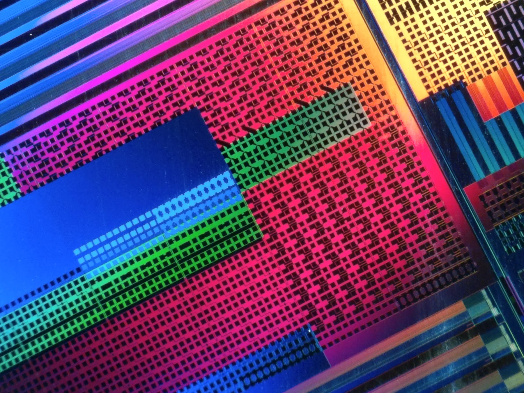
Architecture, RTL and implementation ultimately become physical silicon. These ANKASYS-owned wafer photographs add real semiconductor context without exposing customer layouts or confidential project material.
Discuss architecture, RTL, synthesis, DFT or physical implementation needs with ANKASYS.
END-TO-END SILICON ENGINEERING
ANKASYS supports ASIC and SoC programs across RTL design, synthesis, DFT, physical implementation, signoff and post-silicon validation.
VHDL, Verilog and SystemVerilog RTL development with directed and constrained-random verification using C/C++, SystemVerilog and UVM.
RTL-to-netlist implementation, constraint development, DFT concept development and implementation, and timing closure support.
Floorplanning, placement, clock-tree synthesis and routing, supported by DRC/LVS, STA, formal equivalence, power and IR-drop analysis.
ATE and lab validation, plus PCB, firmware and software engineering for system bring-up.